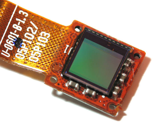
Samsung unveiled a 14nm FinFET process for 144-megapixel sensors at the IEDM forum 2019 in San Francisco. This means going forward the CMOS sensors could be made on the 14nm process. So, to be clear, this new development caters to the process rather than the pixel size.
Here’s how Samsung details the technology and its benefits –
ALSO READ: TRAI Revises Rules for Mobile Number Portability Applicable from December 16
Samsung’s 14nm FinFET Process for Camera Sensors
First things first, for those unaware, CMOS is the image sensor primarily used in cameras be it DSLR or Mobile phone. These are traditionally inexpensive and more power-efficient, but with the caveat of lower quality output.
Samsung researchers underlined the need for the lowest possible voltage which will, in turn, reduce overall power and heat.
Thus comes forth the new 14nm baking for image sensors. In the presentation, they claimed a 144MP capture at 10fps will consume 42-percent lesser juice. Further, a 12MP video recording at 30-120fps will also save up to 37-percent.
ALSO READ: Vivo X30, X30 Pro with Exynos 980 Chip, FuntouchOS 10 and 64MP cameras go official
“CMOS Image Sensor(CIS) products need higher voltage device and better analog characteristics than conventional SOC & Logic products. This work presents newly developed 14nm FinFET process with 2.xV high voltage FinFET device characteristics showing excellent analog and low power digital characteristics comparing to 28nm planar process. Gm is improved by 30% and 67% in FinFET process for NMOS and PMOS, respectively. Rout characteristics increased by 40 times and 6 times over 28nm planar process. Interface state density(Nit) improved by more than 40% and flicker noise characteristics also improved by 64% and 42% for NMOS and PMOS, respectively. Digital logic Transistor ion-ioff performance improved by by 32% and by 211% for NMOS and PMOS, respectively compared to 28nm planar device and the chip power consumption of digital logic functional block reduced by 34% in real Si of 12M pixel product. 14nm FinFET process expected to improve power consumption by 42% in 144M pixel density.“
