

Samsung presents 14nm FinFET process for 144MP image sensors at IEDM 2019

Main Image
  • Like
  • Comment
  • Share

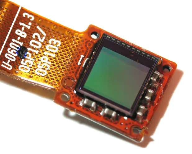
Samsung unveiled a 14nm FinFET process for 144-megapixel sensors at the IEDM forum 2019 in San Francisco. This means going forward the CMOS sensors could be made on the 14nm process. So, to be clear, this new development caters to the process rather than the pixel size.

Here’s how Samsung details the technology and its benefits –

ALSO READ: TRAI Revises Rules for Mobile Number Portability Applicable from December 16

Samsung’s 14nm FinFET Process for Camera Sensors

First things first, for those unaware, CMOS is the image sensor primarily used in cameras be it DSLR or Mobile phone. These are traditionally inexpensive and more power-efficient, but with the caveat of lower quality output.

Samsung researchers underlined the need for the lowest possible voltage which will, in turn, reduce overall power and heat.

Thus comes forth the new 14nm baking for image sensors. In the presentation, they claimed a 144MP capture at 10fps will consume 42-percent lesser juice. Further, a 12MP video recording at 30-120fps will also save up to 37-percent.

ALSO READ: Vivo X30, X30 Pro with Exynos 980 Chip, FuntouchOS 10 and 64MP cameras go official

CMOS Image Sensor(CIS) products need higher voltage device and better analog characteristics than conventional SOC & Logic products. This work presents newly developed 14nm FinFET process with 2.xV high voltage FinFET device characteristics showing excellent analog and low power digital characteristics comparing to 28nm planar process. Gm is improved by 30% and 67% in FinFET process for NMOS and PMOS, respectively. Rout characteristics increased by 40 times and 6 times over 28nm planar process. Interface state density(Nit) improved by more than 40% and flicker noise characteristics also improved by 64% and 42% for NMOS and PMOS, respectively. Digital logic Transistor ion-ioff performance improved by by 32% and by 211% for NMOS and PMOS, respectively compared to 28nm planar device and the chip power consumption of digital logic functional block reduced by 34% in real Si of 12M pixel product. 14nm FinFET process expected to improve power consumption by 42% in 144M pixel density.

Vasan G.S.Vasan G.S.
An inquisitive mind who spends a big chunk of the day keenly tracking every emerging detail and is responsible for quickly passing on important developments to Smartprix followers. He loves to stay in his bubble scripting his destiny involving amazing technology and people with good character, passion, and brilliance.

Related Articles

ImagemacOS 27 Golden Gate Public Beta Available Now: Should You Install It?

Right alongside iOS 27, Apple has pushed out the public beta for macOS 27 Golden Gate, and if you’ve been curious about what Siri AI looks like on a Mac, this is the easiest way to find out without a developer account. This follows three developer betas, and it brings the same Siri overhaul as …

ImageNEFT 24×7 is applicable now and it will be Free of Charge from Jan 1, 2020

Starting December 16, you can transfer money via NEFT anytime you want. Yes, the nationwide electronic fund transfer solution is now available 24×7 as per the new RBI rule. So, funds moved between accounts as well as branches will receive the beneficiary’s account within two hours. Between 12:00 am and 8:00 am this morning, NEFT …

ImageMi CC9e Master Lu Score Shows Snapdragon 665 is a minor improvement over Snapdragon 660

Mi CC9e that launched last night is the first phone with Snapdragon 665 chipset. This is an octa-core processor with a 2GHz clock speed. This chipset was launched back in April succeeding the Snapdragon 660 chip. So obviously, we would want to know how much of an upgrade is it over the former? Well, as …

ImageSamsung Galaxy Z Fold8, Z Fold8 Ultra, and Z Flip8 Cases Leak Ahead of Launch

Samsung’s next-generation foldables are expected to debut at the upcoming Galaxy Unpacked event, and a new leak has now revealed what buyers can expect in terms of official accessories. According to images shared by Android Headlines, Samsung is preparing a wide range of first-party cases for the Galaxy Z Fold8 (wide), the Galaxy Z Fold8 …

ImageSony LYTIA 610 64MP Sensor Announced: RB2x2 OCL, 4K 120fps, Specs & Availability

Sony has announced the LYTIA 610, a new 64MP image sensor for mobile cameras. Shipments to device manufacturers start at the end of June 2026. It is the first sensor in the industry to bring an RB2x2 On-Chip Lens pixel structure into mass production. It primarily targets telephoto and secondary cameras rather than a phone’s …

Discuss

Be the first to leave a comment.

Related Products