
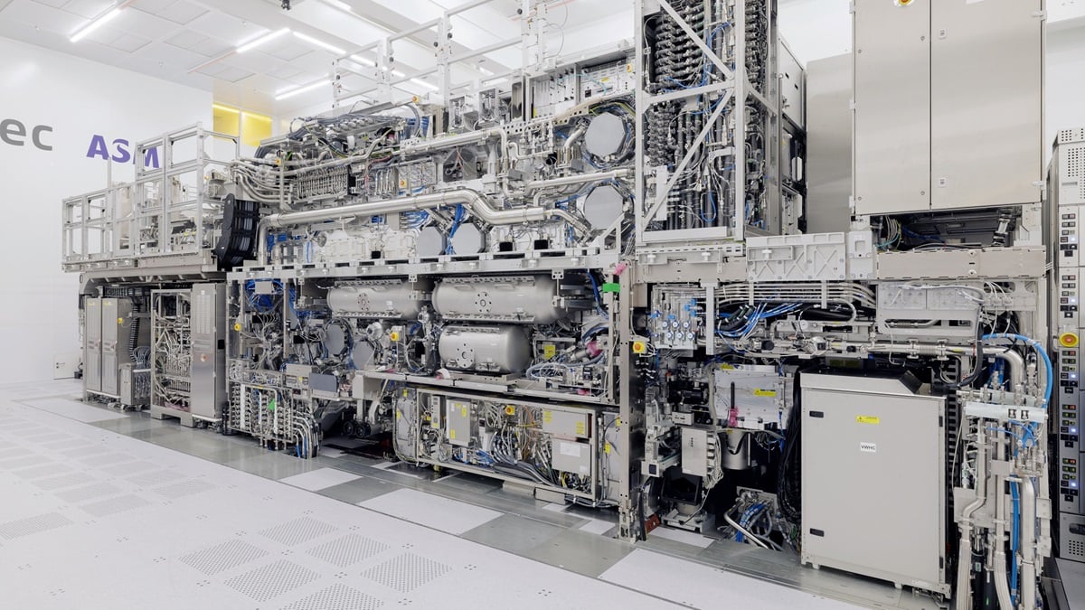
Dutch tech giant ASML shipped its first-ever high-NA EUV lithography tools to Intel in December 2024 which would allow Intel to make smaller chipsets with better performance. However, ASML has been slapped by analyst firms as encouraging customers to buy expensive lithography tools that go upwards of $300 million to $400 million. Cut to now, ASML CEO spoke to Bits and Chips in an interview stating how its lineup of high-NA chipmaking tools is a logical and cost-effective solution available today.
ASML is the EUV machine makers that deal with giants such as TSMC and Intel developing and selling the tools used to make system-on-chips (SoCs). ASML’s latest Twinscan EXE High-NA EUV lithography tools are the next-gen EUV technologies that can mint chipsets smaller than 2nm. The machines typically cost around $300 million to $400 million per unit and use various technologies and peculiarities such as large dimensions and halved reticle size to process smaller chips while sustaining the yield rate.
Analyst firms took a dig on ASML for selling expensive machines to which, ASML replied that they had underestimated the impact using a next-gen lithography machine would bring including cutting down on the cut of double or even quadruple-patterning which leads to higher risks of defects and lower yield rate. Intel’s 10nm chipsets failed due to double-patterning and a lack of robust EUV technology at the time.
For the unversed, low-NA tools that are currently in use, deploy methods such as double patterning to make out circuitry on tiny chips. It begs the question of why would a chipmaker purchase an expensive high-NA EUV machine if the former can do its job properly. However, it all boils down to the increased risk of over-exposing the silicon wafers to double or even quadruple patterning which could lead to defects and lower yield rates.
Note that double patterning isn’t all that bad since TSMC used it across Apple A17 Pro and M3-based chips fabbed on the N3B process and they have outperformed the predecessors. However, the risk remains intact. Additionally, there are also longer production times that chips would have to undergo when exposed twice or more.
ASML has clearly stated that companies can weigh out the pros and cons of upgrading to high-NA EUV machines before deciding. Certain tech giants will commence their research and development in 2024-25 followed by manufacturing in 2025-26 which is when High-NA EUV machines will acquire better cost-to-ROI ratio thanks to their improved technologies and smaller fabrication processes.
You can follow Smartprix on Twitter, Facebook, Instagram, and Google News. Visit smartprix.com for the most recent news, reviews, and tech guides.