
Samsung To Set New Memory Density Standards Soon

Main Image
  • Like
  • Comment
  • Share

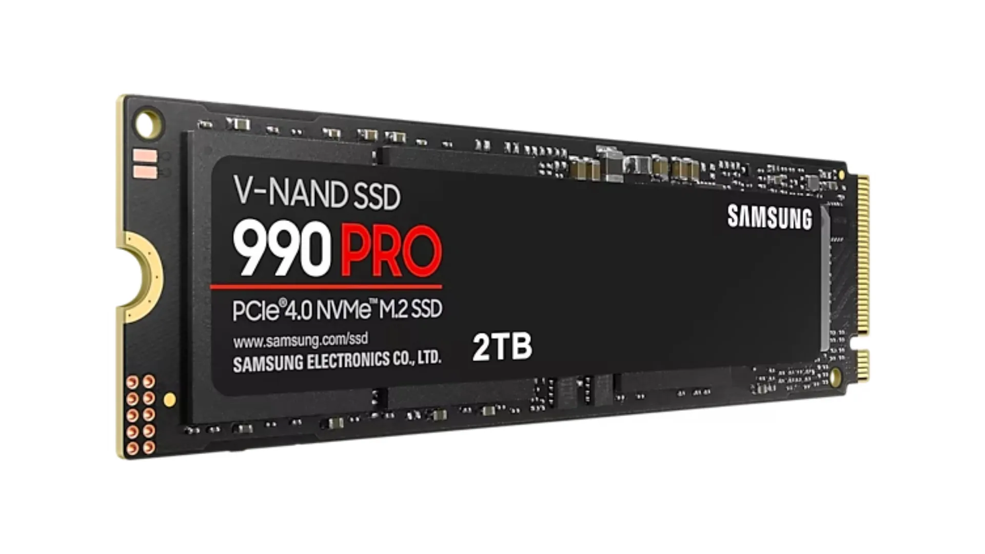
The PCs and laptops we use regularly rely on two key components to function: memory and storage. These components come in shapes and sizes, starting from entry-level chips on affordable models all the way to high-frequency variants that cost more. However, even with the top-of-the-line DRAM and Nand flash chip available, processing data at a massive scale isn’t as efficient. To improve this, Samsung Electronics is working on increasing the memory density of its NAND flash chips and DRAM to “extreme levels.”

Samsung To Achieve Industry’s Highest Level Of Memory Density

Per a report published by KED Global, the 11-nanometer DRAM currently under development at Samsung Electronics “will achieve the industry’s highest level of memory density,” as told by the president and head of the company’s Device Solutions division, Lee Jung-bae. Samsung is planning to achieve this by developing 3D-stacked structures. For V-Nand, the company is working to place more cells on a printed circuit with lower height while reducing interference between cells to condense the size.

As and when the company achieves this breakthrough, it will help the computing industry and all the other fields that rely on data processing, as higher memory density chips will be able to store the same amount of information in fewer chips. In other words, achieving higher memory capacities will be easier using the same number of higher-density DRAM chips.

High-Density Chips Will Benefit AI-Driven Technologies And Services

Although regular users won’t need such performance, it would be highly beneficial for AI-driven technologies and businesses that require high-capacity and low-power memory. A quick example of such companies is Open AI, which needs high data-processing power to train its popular chatbot, ChatGPT. By 2025, the company wants to implement high-bandwidth memory (HBM) modules with a capacity of up to 1 terabyte (or 1,000 gigabytes).

Samsung will apply processing-in-memory (PIM) and processing-near-memory (PNM) technologies to HBM chips, improving data calculation capabilities while increasing the chips’ power efficiency. Another huge claim that could revolutionize the industry is about a petabyte solid state drive or a hardware drive with a million gigabytes, which lower energy consumption than traditional drivers.

The company will showcase more details about its latest semiconductor technologies at the Samsung Memory Tech Day 2023 on October 20, 2023.

You can follow Smartprix on Twitter, Facebook, Instagram, and Google News. Visit smartprix.com for the most recent news, reviews, and tech guides.

Shikhar MehrotraShikhar Mehrotra
Shikhar Mehrotra is a seasoned technology writer and reviewer with over five years of experience covering consumer tech across India and global markets. At Smartprix, he has authored more than 1,700 articles, including news stories, features, comparisons, and product reviews spanning automobiles, smartphones, chipsets, wearables, laptops, home appliances, and operating systems. Shikhar has reviewed flagship devices such as the iPhone 16, Galaxy S25+, and Sennheiser HD 505 Open-Ear headphones. He also contributes regularly to Smartprix’s growing automotive section.

With a deep understanding of both iOS and Android ecosystems, Shikhar specializes in daily tech news, how-to explainers, product comparisons, and in-depth reviews. His DSLR photography in product reviews is recognized as among the best on the team.

Before joining Smartprix, Shikhar wrote for leading publications including Forbes Advisor India, Republic World, and ScreenRant. He holds a Bachelor of Arts in Journalism and Mass Communication from Amity University, Lucknow.

Related Articles

ImageiPhone Duo Repair Costs in India: A Cracked Inner Screen Means a ₹1,49,900 Bill Without AppleCare+

There’s been plenty of excitement around Apple’s first foldable, but as an Apple user myself who had my iPhone 13’s rear glass repaired back in the day, I kept thinking about the bill that could follow a bad drop. Roughly a month after the September 2026 grand unveiling, Apple has published repair costs in India. …

ImageSamsung unveils uMCP memory, a combination of LPDDR5 and UFS 3.1 in one chip

Samsung Electronics has announced a new memory technology for phones called uMCP which stands for UFS-based multichip package. It is an integration of LPDDR5 DRAM with UFS 3.1 NAND flash on one chip. Due to this unified design, uMCP takes less space within phones and should bestow better performance and efficiency. By bringing both memory …

ImageSamsung releases LPDDR5X DRAM with better performance and power efficiency

Samsung Electronics has announced the LPDDR5X DRAM for smartphones, servers, and automobiles. The company calls it the industry-first 14 nm-based 16Gb (Gigabit) LPDDR5X DRAM. Compared to the precursor, it boasts improved speeds and lesser energy consumption. Samsung LPDDR5X DRAM features If the LPDDR5 launched by Samsung back in 2018 was 8Gb in size, the newcomer …

ImageSamsung Announces UFS 5.0 Storage With Up to 10.8GB/s Speeds, Mass Production Set for Late 2026

Samsung Electronics has officially announced its next-generation UFS 5.0 storage solution, bringing substantial improvements in performance and power efficiency as smartphone makers prepare for increasingly demanding on-device AI workloads. According to Samsung, the new storage standard delivers sequential read speeds of up to 10.8GB/s and sequential write speeds of up to 9.5GB/s. That’s more than …

ImageSamsung’s New Laptop OLED Panels Hit 1,600 nits, And Lenovo Is Already Shipping Them

Samsung Display has begun mass production of what it claims is the industry’s first laptop OLED panels to achieve VESA’s new DisplayHDR True Black 1400 certification (1,400 nits in a 10% of the window). For those catching up, it is a standard that requires roughly 40% more peak brightness than its predecessor.  Also Read: Gabit …

Discuss

Be the first to leave a comment.

Related Products